India’s Chip Dreams Take Shape: IIIT Hyderabad Unveils Cutting-Edge FabLab for Semiconductor and Microfabrication Research
India’s semiconductor journey just took a significant leap forward, and the epicenter of this transformation is a pristine cleanroom inside IIIT Hyderabad. With the official inauguration of its FabLab, the institute has positioned itself at the forefront of India’s indigenous efforts in microfabrication, chip characterization, and advanced semiconductor research.
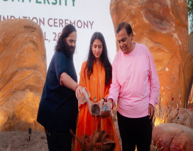
The lab was inaugurated on July 31, 2025, by IIIT-H Director Prof. P J Narayanan, and marks a tangible milestone in India’s broader vision for technological sovereignty. Funded under the Department of Science and Technology’s (DST) Promotion of University Research and Scientific Excellence (PURSE) scheme, the FabLab is more than just a facility—it is a national asset built to nurture homegrown innovation.
FabLab: A Launchpad for India’s Semiconductor Ecosystem
While India continues to be largely dependent on imported semiconductor components, the launch of this lab signals a decisive shift toward self-reliance. Principal investigator and coordinator of the PURSE grant, Dr. Aftab Hussain, captured the significance of the moment:
“This lab is a game-changer. It’s not just about equipment, but about capacity-building—training students, researchers, and regional stakeholders in how to design, build, and characterize semiconductors from the ground up.”
The lab is equipped with a full suite of microfabrication tools, allowing for the development of integrated circuits (ICs), biosensors, bio-actuators, and advanced electronic devices—all within the confines of the campus.
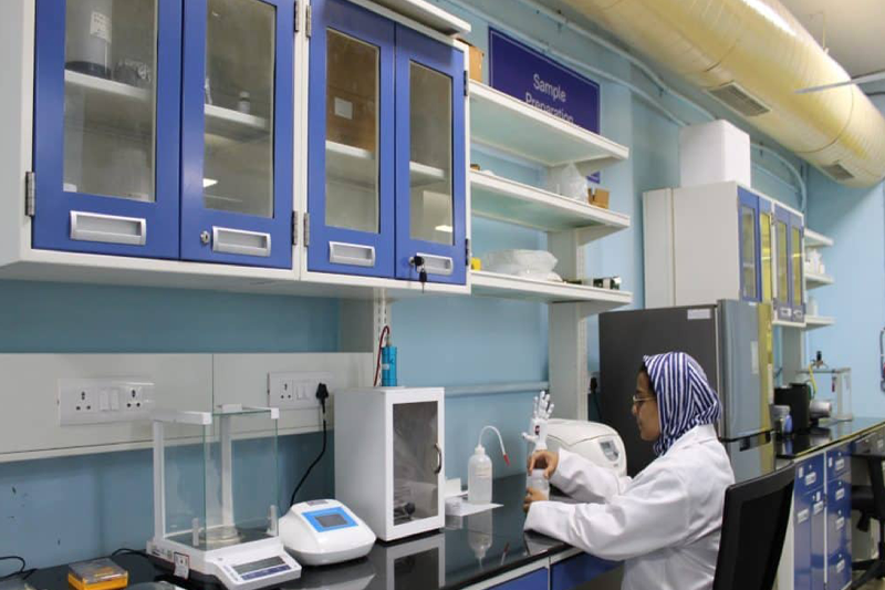
Inside the FabLab: Precision at the Nanoscale
Walking through the FabLab feels like stepping into the future of nanotechnology. This meticulously designed cleanroom houses some of the most advanced semiconductor research tools available in India today:
- UV Lithography Units: For etching micro- and nano-scale patterns onto substrates
- Sputtering Systems & Spin Coaters: To deposit and layer materials with nanometer accuracy
- Vacuum Chambers: Enabling high-precision experiments in controlled environments
- Scanning Electron Microscope (SEM), Energy Dispersive X-ray Spectroscopy (EDS), and Optical Profilometers: Providing deep insight into material properties and surface profiles
But the lab’s true strength lies in its semiconductor IC testing capabilities, particularly at millimeter-wave (mmWave) frequencies—a domain essential for 5G, automotive radar systems, and ultra-fast wireless communication.
The lab features:
- Probe Stations
- Vector Network Analyzers (VNA)
- Vector Signal Generators (VSG)
- Signal Analyzers
- High-bandwidth Oscilloscopes
Together, these tools allow researchers to simulate, test, and validate IC designs with pinpoint accuracy.
Interdisciplinary Research at Its Core
One of FabLab’s most compelling aspects is its interdisciplinary orientation. The lab will serve as a bridge between fields such as:
- Material Science
- VLSI Design
- Biomedical Engineering
- Wireless Communication
This fusion creates fertile ground for innovation, particularly in applications like biosensors for healthcare, next-gen antennas for communication, and smart integrated systems for various industries.
Dr. Hussain emphasized that the FabLab isn’t intended to remain an isolated pocket of excellence:
“We intend to open this facility to external users across the region. This is a shared resource, not a silo.”
Training the Next Generation of Chipmakers
Beyond infrastructure, IIIT Hyderabad is focused on building human capital. The institute will soon roll out specialized courses and hands-on workshops tailored to train students, researchers, and early-stage startups in semiconductor technology.
This approach aligns perfectly with India’s national push toward semiconductor sovereignty, as outlined in the India Semiconductor Mission. As global supply chains remain volatile, the country’s urgency to cultivate local design and fabrication talent has never been higher.
The FabLab’s capacity to train engineers in everything from lithography to mmWave testing makes it a critical educational and research resource not just for IIIT-H, but for India at large.
A Legacy of Innovation Continues
Founded in 1998, IIIT Hyderabad has long held a reputation for pioneering interdisciplinary research with real-world impact. Its work has spanned fields as diverse as:
- Robotics and AI
- Language Technologies
- Earthquake Engineering
- Computational Natural Sciences
- Wireless Communication and VLSI
The FabLab is the natural evolution of that legacy—a physical manifestation of years of research ambition brought to life with world-class equipment and national-level collaboration.
Looking Ahead: Building India’s Silicon Backbone
As India continues to ramp up its semiconductor manufacturing capabilities, hubs like the FabLab at IIIT-Hyderabad will be instrumental in laying the groundwork. These small yet sophisticated ecosystems provide the R&D, talent development, and collaborative innovation needed to support larger manufacturing goals.
A virtual walkthrough of the FabLab is already available online—but its true promise lies beyond visuals. Hidden in the vacuum chambers and etched on silicon wafers are the building blocks of a future where India no longer needs to look abroad for critical tech components.
Between sputtered atoms and high-frequency signals, the foundation for India’s chip-making revolution is now firmly in place.