India Unveils Indigenous Silicon Photonics at IIT Madras, Boosting Semiconductor Self-Reliance
India Advances Semiconductor Sovereignty: Indigenous Silicon Photonics Solutions Launched at IIT Madras
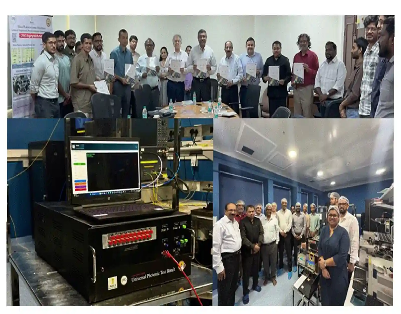
In a decisive stride towards technological self-reliance, India has unveiled indigenously developed silicon photonics solutions at the Indian Institute of Technology Madras, signalling a transformative moment in the nation’s semiconductor ambitions. The launch, led by the Ministry of Electronics and Information Technology (MeitY), underscores a broader national commitment to reducing dependence on imported chip technologies while cultivating a robust domestic innovation ecosystem. At a time when global semiconductor supply chains remain geopolitically sensitive and technologically concentrated, India’s entry into silicon photonics, a frontier field blending optics with semiconductor engineering, marks both strategic foresight and scientific maturity.
Understanding Silicon Photonics: The Technology Behind the Breakthrough
Silicon photonics represents a paradigm shift in chip design, enabling data transmission through light rather than electrical signals. This approach significantly enhances speed, reduces energy consumption and supports the growing demands of high-performance computing, artificial intelligence and next-generation communication systems. Unlike conventional electronics, photonic systems leverage photons instead of electrons, thereby minimising heat generation and latency. The indigenous solutions launched at IIT Madras are poised to align India with global advancements in this domain, with officials noting that the country’s progress is now comparable to international standards.
The Core Innovations: PDK and Photonic Test Engine
The launch comprises two cornerstone technologies, each designed to address critical gaps in India’s semiconductor ecosystem.
Silicon Photonics Process Design Kit (PDK)
At the heart of the initiative lies the Process Design Kit (PDK), a comprehensive toolkit that enables the design and fabrication of photonic integrated circuits. This indigenous PDK includes over 50 verified components, providing a foundational library for engineers, researchers, startups and industry players to develop advanced photonic chips within India. By offering a standardised and accessible design framework, the PDK significantly lowers barriers to entry in chip design, fostering innovation across academic and industrial domains.
Universal Programmable Photonic IC Test Engine
Complementing the PDK is the Universal Programmable Photonic Integrated Circuit (PPIC) Test Engine, a sophisticated platform for testing and characterising photonic and optoelectronic modules. This system enables automated validation of chip performance across a wide range of applications, ensuring reliability and scalability. Together, these innovations form a cohesive ecosystem, spanning design, development and testing, thereby addressing the entire lifecycle of photonic chip creation.
A National Milestone in Semiconductor Self-Reliance
The significance of this development extends far beyond academic achievement. It aligns closely with India’s broader ambition to establish itself as a global semiconductor hub under initiatives such as the India Semiconductor Mission.
Officials have described the launch as a “major milestone in silicon photonics technology sovereignty”, emphasising its role as a shared national facility for the country’s research and development community.
This is particularly pertinent given the strategic importance of semiconductors in sectors ranging from defence and telecommunications to healthcare and consumer electronics. By nurturing indigenous capabilities, India seeks not only to mitigate external dependencies but also to position itself as a contributor to global technological innovation.
Enabling a Broad Spectrum of Applications
One of the most compelling aspects of silicon photonics lies in its versatility. The newly launched solutions are expected to catalyse advancements across multiple domains:
- High-Speed Data Communication: Enhancing bandwidth and efficiency in data centres and telecom networks
- Artificial Intelligence and Computing: Supporting faster and more energy-efficient processing systems
- Quantum Technologies: Enabling secure communication and advanced computational paradigms
- Defence and Aerospace: Strengthening indigenous capabilities in secure and resilient communication systems
Indeed, experts have highlighted that silicon photonics holds potential across both classical and quantum computing regimes, reflecting its transformative scope.
The Role of IIT Madras: A Hub of Innovation
The development of these technologies at IIT Madras is emblematic of the institution’s enduring leadership in cutting-edge research. The solutions have been created under a government-supported Centre of Excellence dedicated to programmable photonic integrated circuits.
Over the years, IIT Madras has consistently contributed to India’s technological ecosystem, including earlier breakthroughs such as silicon photonics-based quantum random number generators and advanced photonic devices.
This latest achievement further consolidates its position as a crucible of innovation, where academia, industry and government converge to address complex technological challenges.
Strengthening the Innovation Ecosystem
Beyond the immediate technological gains, the launch is expected to have a cascading impact on India’s innovation landscape.
Empowering Startups and Industry
By providing indigenous tools and infrastructure, the initiative enables startups and small enterprises to participate in high-end chip design without reliance on costly foreign technologies.
Advancing Academic Research
The availability of a shared national facility encourages collaborative research, fostering interdisciplinary exploration in photonics, electronics and quantum sciences.
Supporting Defence and Strategic Sectors
Indigenous photonic solutions reduce vulnerabilities associated with imported technologies, thereby enhancing national security.
Bridging the Gap with Global Leaders
Historically, the semiconductor industry has been dominated by a handful of countries with advanced fabrication and design capabilities. India’s entry into silicon photonics represents a strategic effort to bridge this gap.
Officials have acknowledged that while the country has made significant progress, the next step involves establishing dedicated fabrication facilities to fully realise the potential of these technologies.
This underscores the importance of continued investment, policy support, and international collaboration in building a comprehensive semiconductor ecosystem.
Challenges and the Road Ahead
While the launch marks a significant milestone, several challenges remain:
- Fabrication Infrastructure: The absence of large-scale semiconductor fabrication units remains a constraint
- Skilled Workforce: Expanding expertise in specialised domains such as photonics and quantum engineering is essential
- Global Competition: Keeping pace with rapid technological advancements in leading economies requires sustained effort
Nevertheless, initiatives such as this demonstrate a clear trajectory towards overcoming these challenges through innovation and collaboration.
A Vision for Technological Sovereignty
The unveiling of indigenous silicon photonics solutions is more than a technological achievement; it is a statement of intent. It reflects India’s aspiration to transition from a consumer of advanced technologies to a creator and exporter of cutting-edge innovations. By integrating design, testing, and research capabilities within the country, the initiative lays the groundwork for a self-sustaining semiconductor ecosystem. It also aligns with broader national objectives of economic resilience, digital transformation and strategic autonomy.
Conclusion
The launch of silicon photonics solutions at the Indian Institute of Technology Madras marks a defining moment in India’s technological journey. As the nation seeks to establish itself as a formidable player in the global semiconductor arena, such initiatives serve as both catalyst and cornerstone. In an era where technological capability increasingly determines economic and strategic influence, India’s foray into silicon photonics signals a future shaped not by dependence but by innovation, ingenuity and self-reliance.